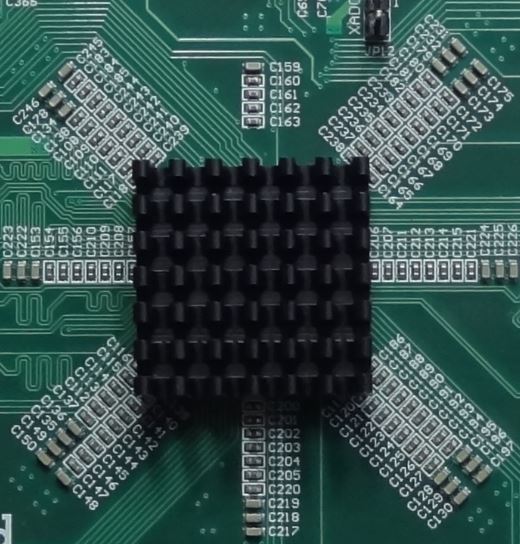
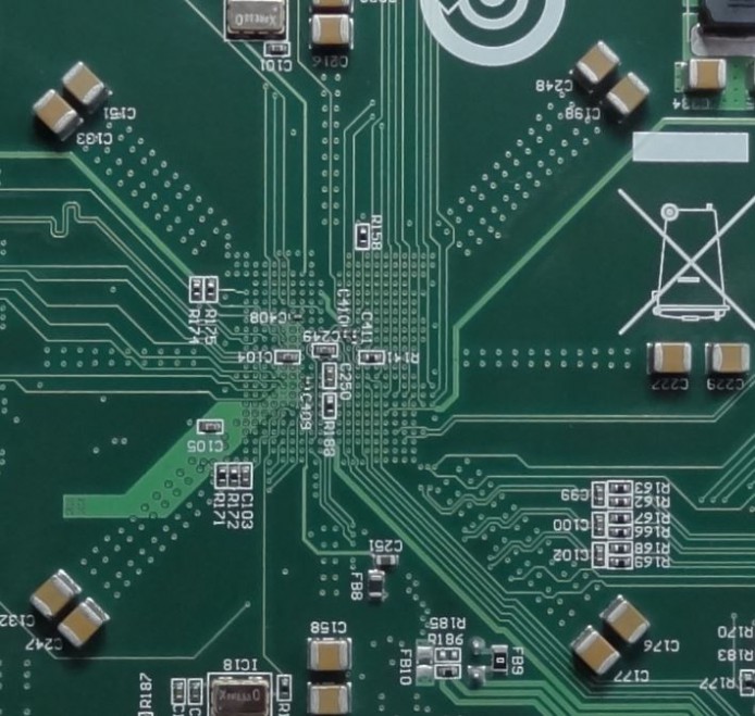
A question came up: Does the Zedboard bypass scheme make sense? The Zedboard is an eval board for the Xilinx Zynq-7000 FPGA. As such it may be nothing special, but when you look at the board you will notice a very interesting pattern of bypass capacitors. And there is a long story on the web page about why the designer thinks this is a good way to do bypass that way for a board like this.
Decoupling power supply is one of the most important topics in signal integrity, so I found this to be an interesting board with a good story. Do you agree with the method used? Is the designer right? Or is it BS? Would you be able to make that distinction if this was in an application note?
I invite your comments below.
PS: If you sign up before the early bird 10% discount on The Nordic SI Week 2014 with Lee Ritchey ends on March 1st, you may win one of these boards. Thanks to Silica for sponsoring this.
UPDATE (Jan 24, 14): I got the board in my hands now, so I could shoot some better pictures of this board from both the top and bottom side.
UPDATE: The results are in. Read about the measurements we did on this funky Zedboard bypass/decoupling capacitor scheme.


 M.Sc.EE, SI Consultant
Also follow the discussion on LinkedIn: http://linkd.in/1gkmSiE (You may need to be part of the PCB Designers group)
I have a two guesses about this disign.
1. Because capacitors are not optimally close to power pins, there is long tracks on a ground plane, where currents flowing through this capacitors interact with return currents of a signal traces located under/above the ground plane. This may be cause of the noise.
2. If we want to measure the noise added with long routes from power pins to capacitors (and its extra inductance) it is strange to measure this noise across capacitors because we exclude the inductance of long routes from measuring results.
As a suggestion for Xilinx for the future, multi chip modules are increasingly common… imagine HF bypassing in the package, and additional easier bypassing outside.
I don’t have the full answer on the design shown, but I like the small caps snaked in and near the center on the bottom. Then if they are the same nets as the larger caps, the larger caps are not as critical.
If you look closely at the Zynq package, you will see discrete caps on the package and I am sure there is also significant bypass both in forms of inter-plane capacitance in the package and on the die.
You can see this at the bottom of this post:
https://www.ee-training.dk/announcement/measuring-bypass-capacitors-on-a-populated-board.htm
I will add some measurements later.
Look at the top side. It has almost no traces! I’d pour the ground plane on the top and double its weight. That would cut the decoupling inductance in half. With buried strip lines on the critical routes, I think I could lay this board out on 6 planes (or maybe 5).