There has been a lot of discussions (on this blog, on LinkedIn and on Electronics StackExchange) about the bypass scheme on the ZedBoard (a Xilinx Zynq FPGA eval board distributed by Avnet/Silica). It made sense to do some actual measurements on the board instead of relying purely on speculations.
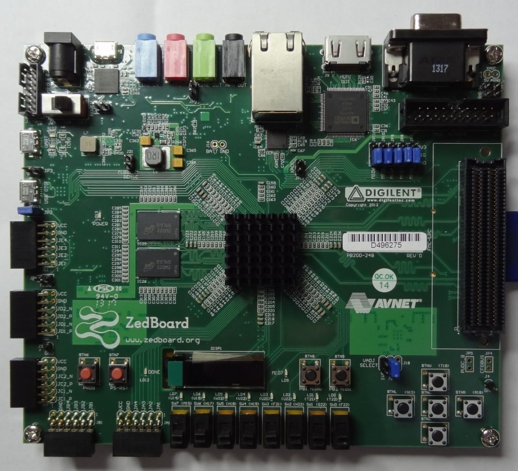 It is clear from the funny placement of bypass caps that the designer did some thinking here and this is all documented in a lengthy word document available on the website.
Measurements
There are two good ways to measure bypass on a circuit board:
- Measuring the impedance versus frequency of the board without power
- Measuring the actual noise on the voltage rails when the board is running
The first method requires two good test points as the measurement has to be done as a 2-port measurement (what the RF guys call an S21 measurement, only we don’t care about the phase). This method has been described in many places including the quick video I did a long time ago.
The second method is actually shown in the lengthy Word document on the ZedBoard website. Unfortunately, the engineer apparently made a few mistakes in the measurement. For one the measurement was done across a bypass cap mounted on the board – as shown later, this filters out a lot of the relevant signal. The oscilloscope bandwidth is only 100MHz which is on the low side – even though the Xilinx User Guide UG 933 explains that external bypass is only required up to 100MHz.
By using the impedance versus frequency method, the results can be compared to other boards that I happen to have in the lab at the moment.
Probing ZedBoard Bypass: not easy
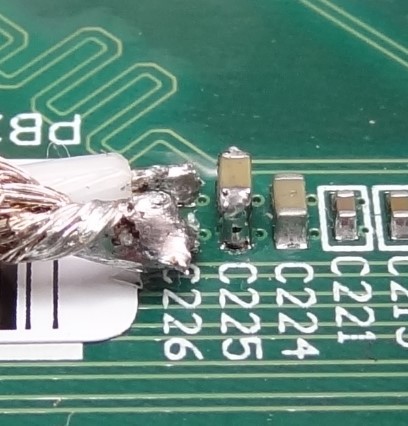
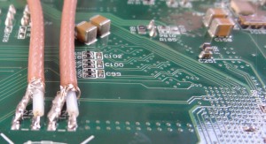
Unfortunately, the board does not have good test points for test probes, so two capacitors were moved and some cut off coax cables were soldered down instead.
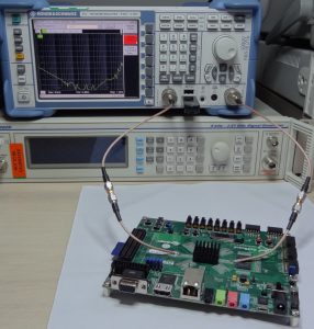
The complete test setup with the ZedBoard looks like this:
Since this board does not have a good power/ground plane pair area but rather something that looks like very wide traces radiating out from the center where the Zynq chip is mounted, a second measurement was done. Four 100uF capacitors are located on the back of the board, and two were easily moved on top of other caps to make room for this connection of the coax cables:
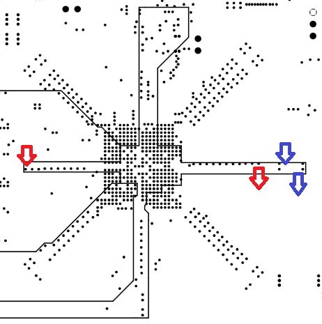
The layout shows the difference between the two measurements:
- Red: Measurement 1 from top side of the board across the bypass row.
- Blue: Measurement 2 from the bottom side of the board in one end of the bypass row.
Here shown in red and blue, with red showing where the signal from the network analyzer enters and exits in the first measurement. The blue arrows show the same thing for the second measurement. This is the power area layer (we are only looking at the 1.0V core voltage to keeps things simple here).
The first measurement looks like
Coax In -> Half the caps -> IC -> Half the caps -> Coax Out
The second measurement looks like
Coax In -> Coax Out -> Half the caps -> IC -> Half the caps
The difference is quite visible in the measurement results. This is how the impedance measurement of the ZedBoard with 35 capacitors (4x100uF, 8×4.7uF, 2×0.47uF, 4×0.1uF, 12×0.047uF, 5×0.01uF but no significant plane capacitance) looks like when measured in the two different ways as shown:
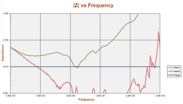 The reality for the chip is going to be somewhere between these two extremes. As can be seen, a more solid power/ground plane pair would make PDN measurements easier to do, even though it may not be strictly required to make a chip with sufficient on-die/on-package capacitance work okay.
Also, a more solid power area would make the exact location of the capacitors less important as can be seen in another blog post on this site.
So this is not an ideal measurement. Sorry (feel free to suggest a simple way to do a better measurement of this). But it does show some of the effects in play here.
Comparison
As a comparison, the measurement points on a client board with a solid ground plane and a good size core power area were moved around and the results are pretty much identical to over 100 MHz as shown. Read the full details about this measurement in a previous blog post. This is another Xilinx Zynq FPGA based board.
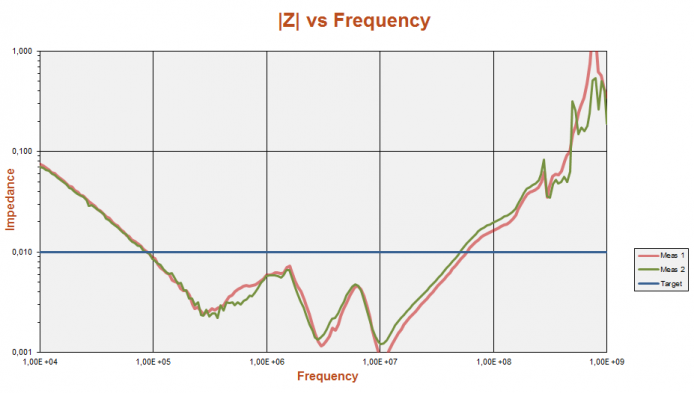 Notice how this board achieves a similar impedance across a wide frequency range with 2/3 the number of capacitors (5x100uF, 6×4.7uF, 12×0.47uF) and a more solid power plane area. Compare this to the ZedBoard bypass.
 M.Sc.EE, SI Consultant
Leave a Reply