• Skip to primary navigation
  • Skip to main content
  • Skip to primary sidebar
  • Skip to footer

EE-Training

Knowledge makes you Curious

  • Home
  • Training Courses
    • Signal Integrity to 56+Gbps with Hands-On Simulation
    • Open the Black Box of Memory
  • References
    • References for Signal Integrity with Hands-On Simulation
    • References for SI Simulation Workshop
    • References for Lee Ritchey: Signal Integrity
    • References for Lee Ritchey: Stackup Design
  • Blog
  • About
    • Terms & Conditions
    • VAT Refund
    • Jobs
  • Contact
You are here: Home » Blog » Tips and tricks

Schmartboard breakout prototyping PCB

February 24, 2020 by Rolf Ostergaard

The hunt for the perfect prototyping breakout boards ended at “Schmartboard” this time. At my first job, we had something we called “mini-mount” in the lab. Lots of them. And we used it to build all kinds of prototypes. Basically, it was a footprint for some SMT part on a thin single layer PCB with thin double-sided tape on the back. This was so convenient for quick mock-ups, prototypes, and when placed on a solid copper plane we could build very high-frequency stuff with this. And they were cheap.

I have been searching for these “mini-mount” things ever since. Not sure what the real name was and where they came from. I never really found anything quite as good.

Recently the hunt was on again as I wanted to help my friend Matt build a super low power mock-up. So I discovered “Schmartboard”:

Schmartboard
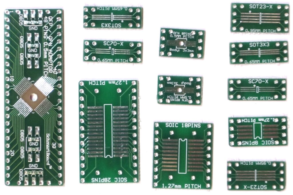
It’s not the same as our “mini-mount” back then. But it’s better in a way – and also worse. And it’s innovative. Let me start by explaining the innovation bit. By putting each (long) pad of the footprint into a groove, even the tiniest SMT parts align easily and can be soldered with ease. This is best shown in this photo:

Schmartboard groove for soldering

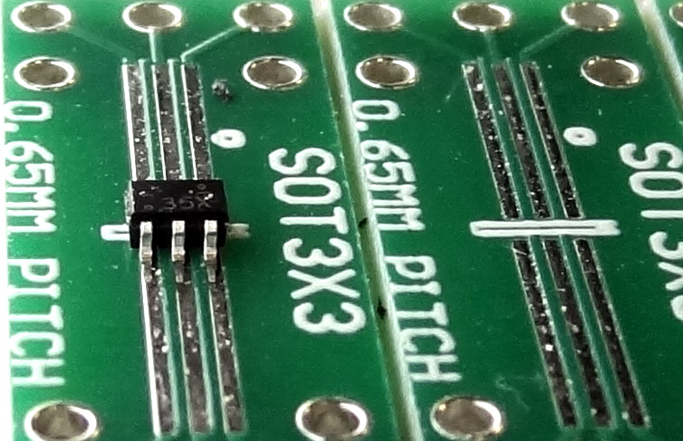
They even add the needed solder onto the trace in the groove so you apply flux and then “push” the solder towards the device and avoid adding too much solder. Hard to explain – try it (or see the video). This concept is pretty smart. I like it.

The good:

  • Easy to solder
  • Versions for all kinds of footprints

The bad:

  • Not exactly cheap
  • Shorts if placed on a copper plane (which I like to use as a common ground plane for SI reasons)

Hope you like it. Maybe not the end of my hunt for the perfect PCB breakout prototyping board, but Schmartboard does come close.

Let me know what you like to use?

PS: Read more of my random tips & tricks here.

Filed Under: Tips and tricks

About Rolf Ostergaard

Rolf V. Ostergaard, M.Sc.EE. has worked with signal integrity in many different projects since working for 3Com in 1998 as a colleague to Lee Ritchey in Silicon Valley. While building a consulting business focused on advanced electronics and embedded software in Denmark, Rolf has been helping numerous companies with signal integrity and power integrity both as design, simulations, coaching, measurements, and troubleshooting. He started conducting training in SI in 2004 and has trained hundreds of engineers, which lead to founding EE-Training to further expand this.
You can hire Rolf to do signal integrity training and consulting worldwide and remote.

Leave a Reply Cancel reply

Your email address will not be published. Required fields are marked *

Get a free SI book

by Lee Ritchey (was $95),
and news from EE-Training

Search

PDNTool

Try pdntool.com and see how a 1-click optimizer might reduce your bypass caps. Read more...

Categories

Latest News

  • Now LIVE: The ultimate memory interface training
  • Online memory course: Mar 1-5, 2021
  • Crosstalk video demonstration for stripline
  • University SI Course – COVID’19 Version
  • Video: Using a Network Analyzer as a TDR
  • Video: PDN Measurement with a Network Analyzer
  • Signal Integrity w/ Hands-On NOW ONLINE May 11, 2020
  • Schmartboard breakout prototyping PCB
  • Remember: Memory course in Copenhagen Feb 5+6
  • Learn Signal Integrity in Ankara Mar 25, 2019

Recent User Comments

  • Peter on Ground bounce demonstration board
  • Rolf Ostergaard on High Speed Via
  • Rolf Ostergaard on Video: PDN Measurement with a Network Analyzer
  • Peter on Video: PDN Measurement with a Network Analyzer
  • Alexander Sharapov on High Speed Via

Contact

EE-Training
Rolf V. Ostergaard
+45 2684 4876
signup@ee-training.dk

QUOTES

“Training worth attending more than pays for itself in added value for you and your project”

“Training is expensive. Good training is even more expensive. No training is the most expensive.”

Rolf V. Ostergaard

M.Sc.EE, SI Consultant
Twitter: @rolfostergaard
LinkedIn: Profile
Resume: CV (pdf)

Copyright 2020. All prices shown are exclusive of VAT. General Terms & Conditions apply.
By using this site with cookies enabled in your browser you consent. Privacy policy.