
How do you make high-speed vias that work at +56Gpbs? Recently a question came up: How big the clearance hole (anti-pad) needed to be for a through-hole via to have acceptable performance with 56Gbps signals on a high layer count board (22 layers / 2.4mm thickness).
I decided to compile all the information I had into a simple to understand text – maybe not the all-time valid definitive guide, but as close as we get just now. Here you go, sorry for the lengthy post, but there is a lot of information to cover. Let me know if you see something wrong or missing.
If you only need one routing layer for the very high-speed signals, the simplest thing may be to use blind laser-drilled L1-L2 vias, which can be as small as about 4mil/100um. This method can also be used for L3, but as laser drilling requires an aspect ratio of about 1:1, those L1-L3 laser vias are as big as the through-hole vias. In the following, I am assuming you need more routing layers and/or want TH vias.
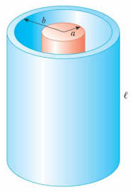
All vias have both capacitance and inductance and will show up on a TDR measurement with an impedance of roughly \(\sqrt{\frac{L}{C}} \) like any other conductor.
Via Inductance
Via inductance is proportional to the length of the via, or rather the length of the via the signal actually has to travel.
If the signal travels along the length of the via from top to bottom, the inductance will be maximum. If the signal enters at the top layer but exits the via halfway down the length of the via, the inductance will be roughly half as big.
Via Capacitance
Via capacitance depends on the size of the via barrel (length and diameter) and the distance to surrounding copper. Roughly the via capacitance is proportional to
 \(1 / ln \left( \frac {drill size} {clearance hole size} \right) \)
Pretty much like the capacitance of a piece of coax:
\(C = l \frac{2 \pi k\epsilon_0}{ln \left( \frac{a}{b} \right) }\)
Note the capacitance does not depend on how much of the via length the signal travels. The capacitance of the via stays the same no matter where the signal enters and exits.
Via Impedance
For a given board thickness, inductance changes, but capacitance stays the same if we change the length of via traveled by our signal.
If we look at the impedance (remembering \(\sqrt{\frac{L}{C}} \)) it is clear that the impedance observed will depend on which layers the signal enters and exits the via.
When trying to break out from under a big BGP package, the size of the clearance hole matters. For a 1mm ball pitch BGA, having more than about 0.8mm clearance holes will practically remove the reference planes, Not good, as the planes are are very important for both traces escaping the BGA and for power supply to the chip.
A 50R High-Speed Via that Works
Fortunately, the following combinations of drill sizes and hole clearances produce close to 50R impedance when used in a 22 layer board with thickness around 2.4mm.
| Drill hole | 0.25 mm (10 mil) | 0.3 mm (12 mil) |
| Capture pad | 0.55 mm (22 mil) | 0.6 mm (24 mil) |
| Clearance hole | 0.75 mm (30 mil) | 0.8 mm (32 mil) |
But only if the full via length is used. That is the signal travel from the top layer (where you place the “dogbone” BGA pad to via connection) and down to layer “N-1” where the signal will exit for routing.
Here is how this looks on the top layer and on an inner plane layer for the two drill sizes (0.25 mm and 0.3 mm drill). Note how much of the plane is still there to provide a reference for the break-out traces on the inner layers.
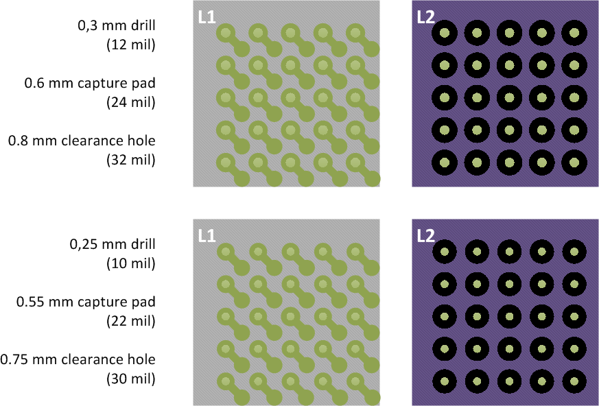
If you want to use this with another board thickness, the values should still work reasonably well as both capacitance and inductance scales with the board thickness. If you use a thinner board you may be able to use a thinner drill, which will change the picture somewhat.
High-Speed Via Measurements
The values given here are a starting point. This has worked well on several boards, but you should make sure they work for you. Three methods exist:
- Measurement on test boards
- Full 3D simulation
- Approximation
Measurements are recommended, as this takes everything into consideration. Make a series of vias with the same drill size and different clearance hole size. Measure all with a TDR (or VNA) and pick the best combination. Make sure you have a well-matched transition from the TDR probe to the board.
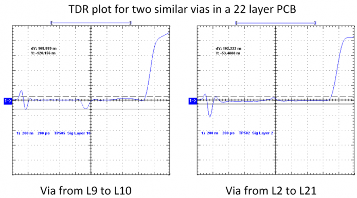
Here is just such an example of two 0.3 mm drill hole vias in a 22L board. Look for the effect of the high-speed via in the middle of the TDR-plot. The one on the left is clearly too capacitive (negative dip), which can be explained by the fact that the signal only travels from L9 to L10 on this via. The one on the right is almost invisible, as the signal travels almost from top to bottom (L2 to L21) in this via.
Full 3D simulation is reserved for those with access to – and a lot of experience in using – the (expensive) tools.
An approximation is also sometimes a useful technique. Cory Ceitz shows how he builds an approximation to his differential via described on the blog. The idea is worth following, even though the concept of differential vias may not be worth the effort (more on this later).
Non-Functional Pads
To keep the capacitance down to the levels assumed here, all non-functional pads are removed from the high-speed via. This is standard practice for high-speed boards and should not pose any problems.
Back-drilling
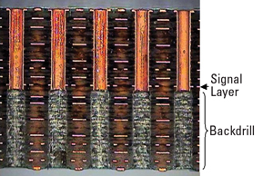 If the routing is so dense that more routing layers are needed, signals may need to exit at other layers than the ones very near the bottom of the board. This is where you may have to use back-drilling on selected vias to remove the bottom (unused) part of the via. This will reduce the capacitance of the via to balance the reduced inductance, keeping the impedance around 50R.
Differential Vias
There is a lot of advice about how to make “differential vias”. This is really a waste of time and effort if you just view the two separate traces of a differential pair as two single-ended traces that happen to carry almost exactly opposite signals. When the traces are routed to have very little coupling, the same goes for the vias. No coupling is required or desired.
Grounding Vias
Many app notes will talk about the need for “grounding vias” near the high-speed vias. The example shown here comes directly from one of many app notes on the subject:
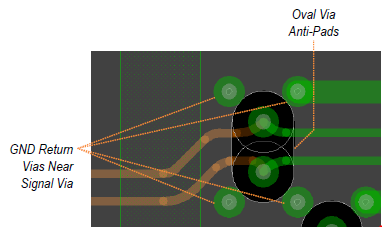
Measurements made on real boards show these extra ground vias to provide no additional benefit visible on a TDR plot. They may be required if you want to do 3D simulation, and don’t want to model the effects of the full low impedance power distribution system.

Note: this image also shows a “differential via”, which is not really worth it either. Read more about why you don’t need grounding vias or stitching vias.
Lumped Element Model
The electrical signal travels at around 145 mm/ns, making a 2.4 mm via about 15 ps “long” in the time domain. With today’s technology, even at 28 GBps, getting any edge faster than maybe 30 ps out of a package and onto a PCB trace is not realistic.
So the edge of even very fast signals will be “smeared” out over the length of the via as it passes through the high-speed via. This is the reason we can safely look at capacitance and inductance as just two elements, with all the tiny effects just lumped into those two numbers. Also note that at these high speeds, it’s really stretching it a bit to talk about edges, as the signals look more like sine waves.
 M.Sc.EE, SI Consultant
how to reduce return current in pcb?
Thanks for reading – not sure I understand your question? Why would you want to reduce return current?
where does signals return current flow in pcb and how to minimize?
The easiest way to reduce return current (still not sure why you want to do that?) is to reduce the forward current as the two must be equal.
thank you
Really interesting post. Thanks for posting!
Another post on how, when, and why return path vias aren’t useful might be very interesting. Since this is counter to “received wisdom” any measurement results you could show would also be valuable. In particular I wonder if it applies as well in low-layer-count boards (4-8 layers) as it does in the high-layer-count boards you seem to work with.
Yes it’s in the works. I want to do this right, so I need some time to format the measurements and explain how they were done. My understanding is that “gnd vias” may be important for simulation – not for the real world 🙂
For 16L to 24L there is virtually no difference as the board thickness just goes up from around 1.6mm to 2.4mm (very rough numbers). For low layer count boards there should be no difference either, but I have no experience with 25+ GBPs on say 8L boards.
It’s an easy measurement to do if you have a TDR and a trace with “gnd vias”. Do a plot before and after you drill out the “gnd via” (don’t forget to send me the two plots).
Hi Rolf,
Very informing article. I have a problem which I am strugling to solve. I do not have this expensive 3D modeling tools. Could you please help. I am connecting stipline (layer3) which is 1mm below top layer (layer1) using via of 0.3 mm in diameter running from top to bottom (layer1 to layer4, the via drill size is 0.4mm with 0.05mm plating thckness) to microstrip on layer1. Layer4 and layer2 are groundplanes. The total 4 layer PCB thickness is a standard 1.6mm. The via pad diameter is 0.6mm. The DK of the dialecric is 4.6 (standard FR4 laminate). What should be the clearance from the via pad to groundplane in order to achieve via impedance of 50ohm?
Thanks and regards,
Valamer
I have question for differential ground vias section described in this article. It suggested that differential signals be routed as two single ended signal with no or little coupling with each other and also you are suggesting that differential ground vias are not required. So are you suggesting indirectly that even single ended signals changing reference plane do not require return vias? And if they are required then will it not be contradictary to what you have suggested that routing differential signal as two single ended signals with no ground vias while changing reference planes.
Yes. But make sure the PDN impedance is low… Maybe use http://www.pdntool.com to help in that design 🙂
I did not understand your answer fully. When reference planes are connected with vias which means both are either ground planes or power planes. So still my question is whether such stitching visa are required or not?. As per your article you are suggesting that they are not required even for single ended signals. Let me know if I have interpreted it wrongly.
Sorry if it wasn’t clear. I have not used stitching vias the last 18 years and do not see why you would need that. But I always have closely coupled pwr/gnd planes and engineer the PDN for low impedance. If you don’t do that – you have a different situation (and other, much worse, problems – or a lot of time).
Thanks for Clarification. Do you think can you provide any theoretical background for why such vias (stitching or return vias) are not important. I’m sure if your measurements concludes that no such vias important then it might also be easy to prove in theory as well for any simple configuration (that can be considered for theoretical explanation). Please do not take my comments in negative way but there is always has been theoretical explanation behind most of SI related issue (for e.g. why controlled impedance, crosstalk etc.) and unless you provide the correlation between measurements and its theoretical explanation (at-least for with some simple example) it would be difficult for me to accept.
If you think about how we always design a very low impedance between pwr/gnd planes in the board as part of the PDN and then compare that to the roughly 1nH/mm inductance of a via, I think you can make the “theoretical” explanation also. Did that help?
Thanks for sharing this post.
I was checking the values you provide for a 50R vias with the Saturn PCB toolbox.
The impedance I get is around 35R.
I suppose it’s based on a different model. Do you think this via calculator is not correct? Is there any other via calculator available?
Thanks,
jesus
It’s a compromise between matching impedance and having enough web left in the power planes for a low inductance power supply. This does the job very well. You really can’t pull the Cu further away from the vias or your PDN will suffer.
Thank you for sharing.
Could you please recommend a software solution for Full 3D simulation.
Best regards,
Alex
Hmmm… How about I recommend you do test boards as a faster, cheaper, and much more reliable way?
I know it sounds counterintuitive, but I think you will realize it really is a good option when it comes to something as complex as 3D simulations.