• Skip to primary navigation
  • Skip to main content
  • Skip to primary sidebar
  • Skip to footer

EE-Training

Knowledge makes you Curious

  • Home
  • Training Courses
    • Signal Integrity to 56+Gbps with Hands-On Simulation
    • Open the Black Box of Memory
  • References
    • References for Signal Integrity with Hands-On Simulation
    • References for SI Simulation Workshop
    • References for Lee Ritchey: Signal Integrity
    • References for Lee Ritchey: Stackup Design
  • Blog
  • About
    • Terms & Conditions
    • VAT Refund
    • Jobs
  • Contact
You are here: Home » Blog » Vias

Ground vias around signal via

October 20, 2014 by Rolf Ostergaard

There has long been a debate going on in the SI community on the need (or not) for ground vias or “stitching vias” near signal vias for high-speed signals. These days you can follow a very interesting and well-behaved debate on the SI-LIST email reflector about just this issue:

http://www.freelists.org/post/si-list/AW-Ground-vias-around-signal-via,21

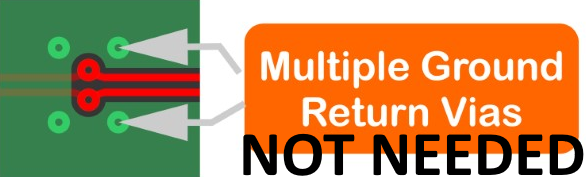
Reading between the lines and balancing the arguments and data provided combined with personal experience from practical design work and my knowledge about the people debating this, I think the conclusion still holds that:

If you have a solid PDN design with low impedance across frequencies,

and

if you have roughly a 1 inch grid of Gnd/Vcc vias (which you will have more or less automatically from bypass caps, IC’s etc),

you do not need to place additional ground vias / “return path vias” / “stitching vias” near signal vias at least up to 28 GBps signaling as used by modern FPGA’s etc.

I am following the debate to see if I can see solid proof that this does not hold. Also, read about high-speed vias here.

Ground vias not needed

Lots of boards I have been involved in are doing just fine without any ground vias around the signal vias. When you think about it, it’s not a big surprise these vias are not helping the return path impedance for the higher frequencies. Basically the inductance creates an impedance of 1/(2*pi*f*L) and the capacitive effect (parasitic or intended) creates an impedance of 2*pi*f*C. As we go up in frequency, the capacitive return path wins and easily gets to a low enough impedance. Adding a ground via is simply not effective at the higher frequencies.

The inductance of a via is a bit less than 1nH per mm the signal has to travel. Even with a thin pre-preg/laminate of 0.1mm, this is about 1/(2*pi*14GHz*0.1nH) = 2 mOhm. A 1pF capacitance will give an impedance in the same order of magnitude. The area needed at that spacing to form a capacitor of around 1pF is in the range of 2x2mm.

Let me hear your take on this?

Share this:

  • Click to email a link to a friend (Opens in new window) Email
  • Click to share on LinkedIn (Opens in new window) LinkedIn
  • Click to share on Reddit (Opens in new window) Reddit
  • Click to share on Bluesky (Opens in new window) Bluesky

Filed Under: Vias Tagged With: vias

About Rolf Ostergaard

Rolf V. Ostergaard, M.Sc.EE. has worked with signal integrity in many different projects since working for 3Com in 1998 as a colleague to Lee Ritchey in Silicon Valley. While building a consulting business focused on advanced electronics and embedded software in Denmark, Rolf has been helping numerous companies with signal integrity and power integrity both as design, simulations, coaching, measurements, and troubleshooting. He started conducting training in SI in 2004 and has trained hundreds of engineers, which lead to founding EE-Training to further expand this.
You can hire Rolf to do signal integrity training and consulting worldwide and remote.

Leave a Reply Cancel reply

Your email address will not be published. Required fields are marked *

Get a free SI book

Right the First Time
by Lee Ritchey (was $95),
and news from EE-Training

Subscribe below!

Search

PDNTool

Try pdntool.com and see how a 1-click optimizer might reduce your bypass caps. Read more...

Categories

Latest News

  • The ultimate memory interface training course live in Copenhagen June 2-4, 2025
  • How we got un-hacked
  • Free IBIS Simulator: KiCAD 8?
  • Online memory course: Mar 1-5, 2021
  • Crosstalk video demonstration for stripline
  • University SI Course – COVID’19 Version
  • Video: Using a Network Analyzer as a TDR
  • Video: PDN Measurement with a Network Analyzer
  • Signal Integrity w/ Hands-On NOW ONLINE May 11, 2020
  • Schmartboard breakout prototyping PCB

Recent User Comments

  • Noelia Scotti on Free IBIS Simulator: KiCAD 8?
  • Vikram Mane on Free IBIS Simulator: KiCAD 8?
  • Peter on Ground bounce demonstration board
  • Rolf Ostergaard on High Speed Via
  • Rolf Ostergaard on Video: PDN Measurement with a Network Analyzer

Contact

EE-Training
Rolf V. Ostergaard
+45 2684 4876
Denmark

QUOTES

“Training worth attending more than pays for itself in added value for you and your project”

“Training is expensive. Good training is even more expensive. No training is the most expensive.”

Rolf V. Ostergaard

M.Sc.EE, SI Consultant
Twitter: @rolfostergaard
LinkedIn: Profile
Resume: CV (pdf)

Copyright 2025. All prices shown are exclusive of VAT. General Terms & Conditions apply.
By using this site with cookies enabled in your browser you consent. Privacy policy. CSR policy.