Figuring out how to simulate ground bounce, Vcc bounce, SSN, SSO (or whatever you want to call it) is not trivial – this is a step-by-step guide to doing Hyperlynx SSN simulations right. This being so difficult is actually a shame, as it can very well be the most significant factor in your signal integrity analysis. This should be (and someday it will be) as easy as simulating reflections, crosstalk, etc.
But first let me explain what I mean by SSN (Simultaneous Switching Noise is also called Ground bounce or Vcc bounce), as there are different uses of the term. The basic premise is that we start with a very solid power distribution system (PDN), so there is a nice and sufficiently low impedance across the frequency range of interest. This is build up between two coupled planes in the board and this is where the IC connects through a set of vias (and maybe some BGA pad “dogbones”). Some want to include PDN effects in the SSN term, but I prefer to keep those terms separate.
With this premise, the following simulation looks trivial (1.65V is half the 3.3V supply voltage):
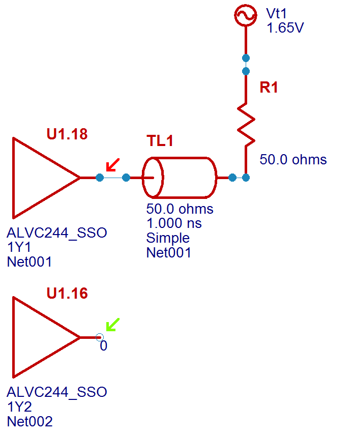
The top output driver is clocked at some frequency – the lower one (U1.16) is set to “stuck low”. Now, what would you expect at the output of the lower one?
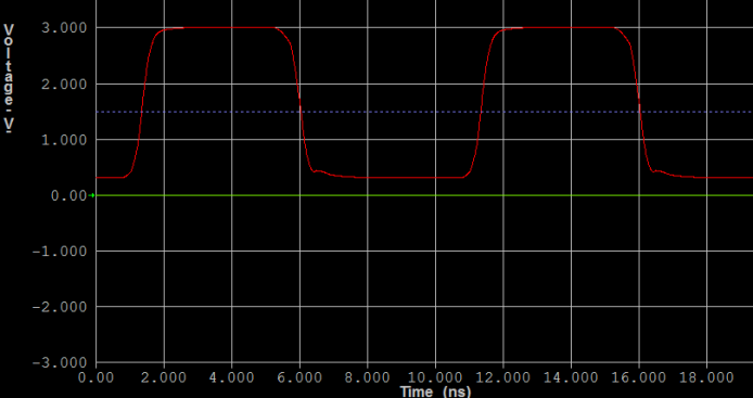
Unless you do some voodoo to the IBIS model file, all you will see for the lower output is a flat line at zero volts. Like this (red is the upper driver output; green is the lower output driver “stuck low”):
Why is this wrong? Well because of SSN.
The Vcc and Gnd connection between the IC pin and the die has some inductance – and across that inductance, we will have a voltage whenever the current changes. This follows the simple formula: U = L * di/dt.
Whenever the output of the top driver output changes, some current will flow through the shared Vcc or Gnd connection of the IC. For the high-to-low edge of the U1.18 output, this current will run through the ground bond wire and IC pin and create a voltage difference between the ground pad on the die and the ground plane in the PCB. This is what I call ground bounce or SSN. Same but opposite for Vcc bounce.
If we think of the simulators ground or 0V point as connected to the ground plane in the PCB, the “stuck-low” output of U1.16 should then show something different than a flat line at zero. Doing Hyperlynx SSN simulations is not that simple.
How do we get Hyperlynx to do so? Well, this requires some modifications to the IBIS file. Here are the steps:
Identify the Power Pins
This is a very simple IC (on purpose to keep confusion to a minimum) with only one power and one ground pin. So open the IBIS model file (which is just a plain text file) in a suitable editor and locate the pin section for the package of interest.
[Pin]    signal_name   model_name          R_pin       L_pin       C_pin
|
1           1NOE       ALVC244_IN          4.200e-02   6.336e-09   8.650e-13
2           1A1        ALVC244_IN          4.300e-02   5.542e-09   8.670e-13
3           2Y4        ALVC244_OUT         3.400e-02   4.714e-09   7.320e-13
4           1A2        ALVC244_IN          3.400e-02   4.377e-09   5.910e-13
5           2Y3        ALVC244_OUT         3.600e-02   4.130e-09   5.330e-13
6           1A3        ALVC244_IN          3.500e-02   4.111e-09   5.300e-13
7           2Y2        ALVC244_OUT         3.400e-02   4.284e-09   5.830e-13
8           1A4        ALVC244_IN          3.400e-02   4.634e-09   7.260e-13
9           2Y1        ALVC244_OUT         4.000e-02   5.518e-09   8.650e-13
10          GND        NC                  4.300e-02   6.349e-09   8.660e-13
11          2A1        ALVC244_IN          4.100e-02   6.281e-09   8.610e-13
12          1Y4        ALVC244_OUT         4.500e-02   5.561e-09   8.680e-13
13          2A2        ALVC244_IN          3.300e-02   4.778e-09   7.420e-13
14          1Y3        ALVC244_OUT         3.500e-02   4.414e-09   5.960e-13
15          2A3        ALVC244_IN          3.500e-02   4.110e-09   5.330e-13
16          1Y2        ALVC244_OUT         3.600e-02   4.130e-09   5.330e-13
17          2A4        ALVC244_IN          3.400e-02   4.377e-09   5.910e-13
18          1Y1        ALVC244_OUT         3.400e-02   4.714e-09   7.310e-13
19          2NOE       ALVC244_IN          4.300e-02   5.569e-09   8.680e-13
20          VCC        NC                  4.200e-02   6.308e-09   8.640e-13
Two things are important here:
- Find the parasitic package induction: 6.35nH for Gnd and 6.31nH for Vcc in this case. You can also find the DC resistance and the parasitic capacitance.
- Make sure the 3rd column reads NC for the Vcc and Gnd pins.
You may want to change the name of the IBIS file when you save it – but remember to change the file name reference in the file as well when you do that.
Create a Spice Sub-Circuit
Now create a plain text file with the Spice simulation lines to define these parasitic elements. Here we place it in a file called “pwrSupply.inc” like this:
* Power supply circuit with package parasitics for pins 10, 20
.subckt  pwrSupply_3v3_with_parasitics  pwrref  gndref

Vgnd  p10  0  DC=0
Vpwr  p20  0  DC=3.3

C_p10_pkg  p10     0       C=8.6600000e-013
L_p10_pkg  p10     p10_RL  L=6.3490000e-009
R_p10_pkg  p10_RL  gndref  R=4.3000000e-002

C_p20_pkg  p20     0       C=8.6400000e-013
L_p20_pkg  p20     p20_RL  L=6.3080000e-009
R_p20_pkg  p20_RL  pwrref  R=4.2000000e-002

.ends
This simple Spice circuit describes the two power pins and their associated bond wires – basically everything from pin to die. You can see it’s a crude description, but enough for many purposes – and this is all the information most IBIS files have. Lumped element R/L/C models for each pin.
Put Circuit Call in the IBIS file
Back in the IBIS file, you need to call this Spice sub-circuit and define which outputs are connected to these power rails. To simplify things, we only define this for the two outputs on pin 16 and pin 18:
[Node Declarations]
pu_ref
pd_ref
[End Node Declarations]
|
[Circuit Call] pwrSupply
Port_map  Vcc_pad  pu_ref
Port_map  Vss_pad  pd_ref
[End Circuit Call]
|
[Circuit Call] ALVC244_OUT
Signal_pin 16
Port_map  A_signal  16
Port_map  A_puref   pu_ref
Port_map  A_pdref   pd_ref
Port_map  A_pcref   pu_ref
Port_map  A_gcref   pd_ref
Port_map  A_gnd     pd_ref
[End Circuit Call]
|
[Circuit Call] ALVC244_OUT
Signal_pin 18
Port_map  A_signal  18
Port_map  A_puref   pu_ref
Port_map  A_pdref   pd_ref
Port_map  A_pcref   pu_ref
Port_map  A_gcref   pd_ref
Port_map  A_gnd     pd_ref
[End Circuit Call]
You can place this right after the pin assignments in the IBIS file. All it does is really connect the power rails of the two I/O cells for pin 16 and 18 to the two new nodes called pu_ref and pd_ref – and connect those two nodes to the Spice sub-circuit.
Define the Spice Circuit Ports
As the last step we can add the definition and parameter mapping of the new Spice sub-circuit file like this:
[External Circuit] pwrSupply
Language SPICE
Corner  typ  pwrSupply.inc  pwrSupply_3v3_with_parasitics
Ports  Vcc_pad  Vss_pad
[End External Circuit]
That’s all. We are now ready to simulate the original simple schematic with the full SSN or Ground/Vcc-bounce effect.
Simulation Results
This is how the simulation of the same circuit looks now:
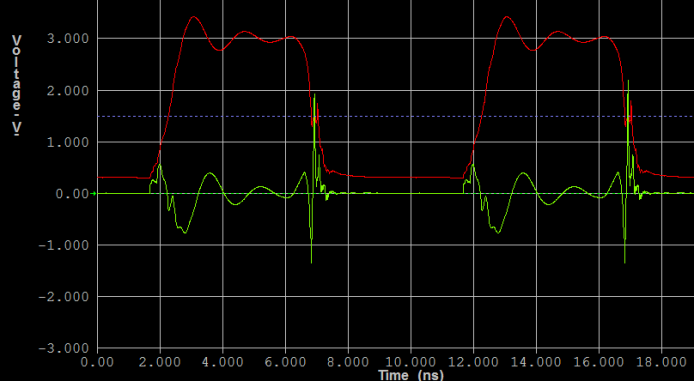
Notice the difference in the green curve (the “stuck low” output)?
And the red curve is impacted quite a bit as well… Almost to the point where you question the validity of the simulation. And you should. So the next step is to scrutinize the simulation setup – and verify it with measurements.
Capacitance
One of the things that can make this Hyperlynx SSN simulation come out as if the part is completely useless because of excessive SSN is the complete lack of die and package capacitance between power and ground. It is very difficult to imagine the die not having at least some capacitance between power and ground.
The good thing about simulators is that experiments are easy to do and free. Let’s try to add 10pF between power and ground at the die and see what happens. To do this, add this line to the Spice file:
R_p20_pkg p20_RL pwrref R=4.2000000e-002
C_die gndref pwrref C=10e-12
.ends
Now run the simulation again to see how much of an effect this has:
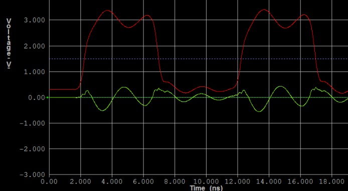
Quite a dramatic effect. This shows how important on-die and on-package capacitance really is. And it also highlights how bad IBIS models are in predicting SSN at the current stage.
How do you think it would look, if someone actually hooked this up on a board and did some measurements? Comment below.
Disclaimer: This is written for Hyperlynx 9.1 – expect SSN simulations to get easier as tools and models evolve. This method is only useful for Hyperlynx – other IBIS simulators have different ways of doing this.
 M.Sc.EE, SI Consultant
Leave a Reply