How about measuring the Power Distribution Network – or PDN – on a populated board? The post on the importance of the distance between the measurement points used when measuring the impedance of all the bypass capacitance on a board triggered another round of questions. Good. One of them is: Why not do a populated board PDN measurement?
Like this:
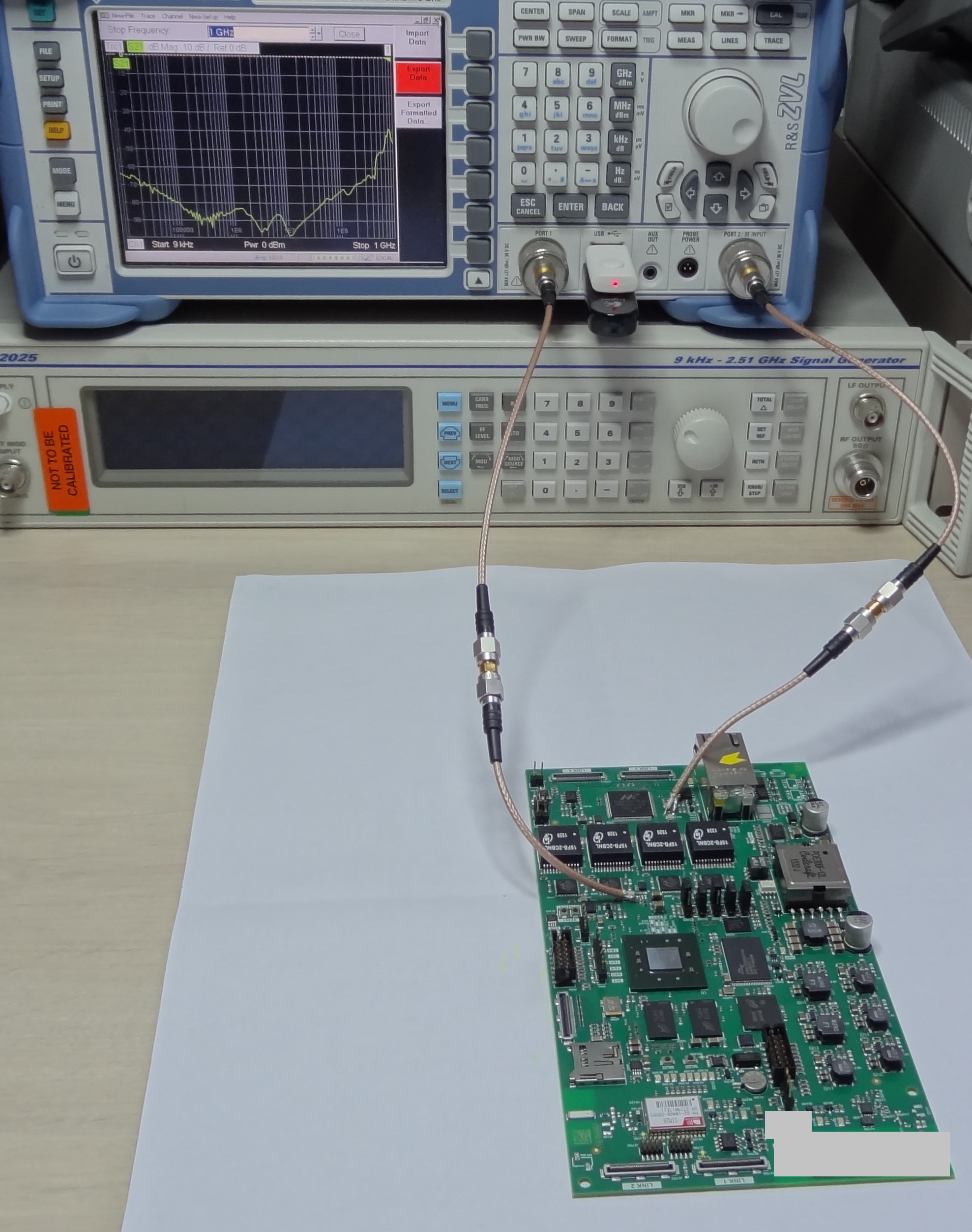 And indeed that is a great idea if that is what you have. In this case, the client was nice enough to provide both this fully populated board and a board with only the bypass caps mounted, so it was very easy to do a comparison.
The RF output in the network analyzer is set to 0dBm. But since the generator is 50R and the impedance between power and ground is maybe 0.01R, the signal is attenuated around 500x and such a small voltage is harmless to the other parts on the board.
Since there is going to be some additional capacitance in the IC packages on the fully populated board, we would expect the impedance to be lower when measured for the populated board versus the “caps only” board.
Results
And that is exactly what we see. Here is the result of the two boards. The red curve shows the effect of the board and its 23 capacitors (5x100uF, 6×4.7uF, 12×0.47uF) only. The green curve shows the effect of this plus the Xilinx Zynq IC with it’s on-die and on-package capacitance.
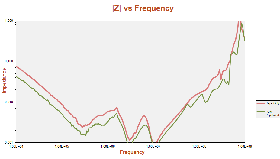 Remember that above about 100 MHz, the results are not really interesting as the impedance is dominated by board resonances. This is about where we see the two small dips on the green curve. Those are most likely coming from the small capacitors on the package substrate.
Also, notice that the impedance at the lower frequencies will be lower when the board is powered up due to the active regulation of the power supply which may effective up to 10s of kHz.
(Note: The measurements are done here only for the 1.0V core voltage supply to the Xilinx Zynq FPGA.)
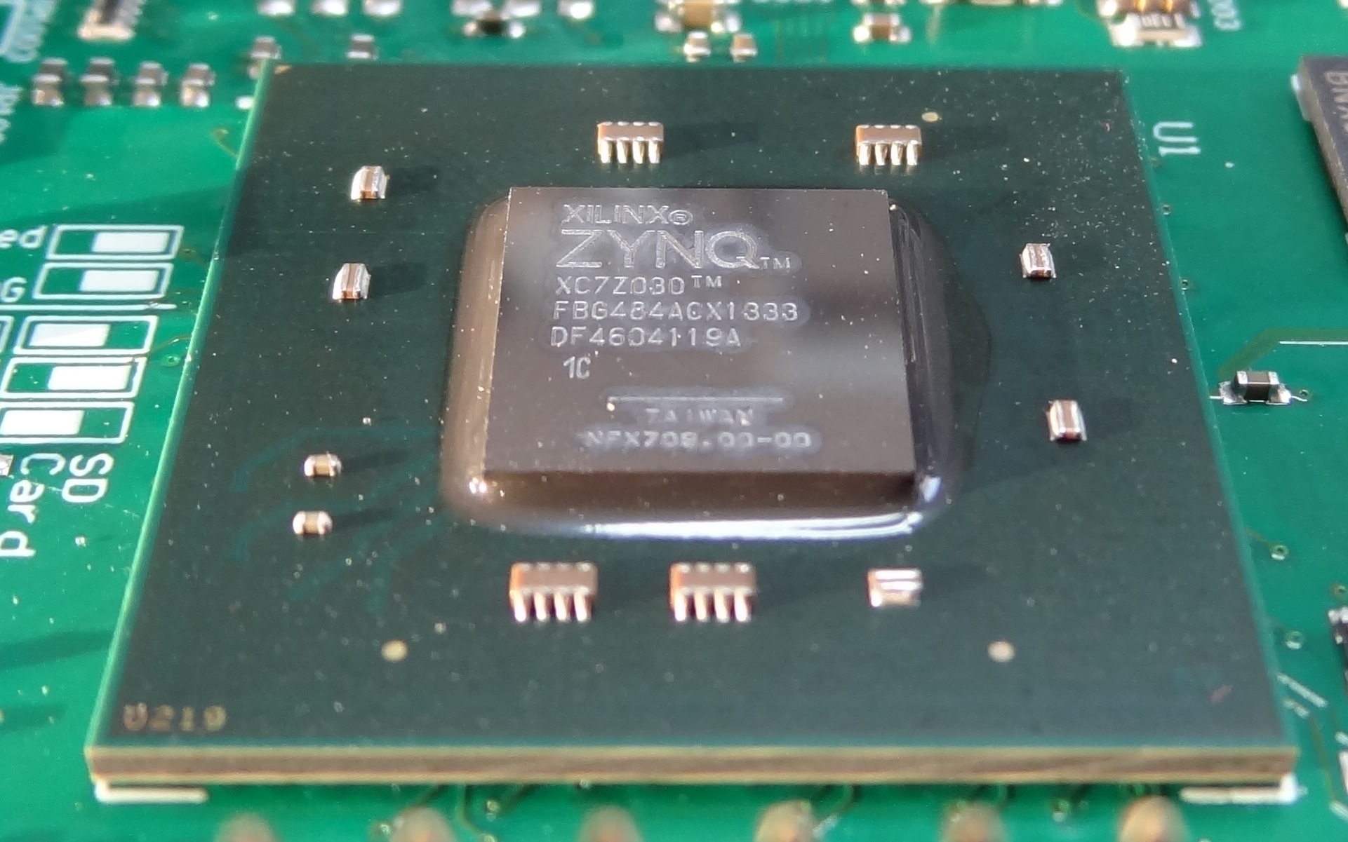
Looking closely at the FPGA chip it is clear that capacitance has been integrated at least at the package level:
 With the FPGA package and die capacitance in place, it would be nice to be able to take advantage of that when designing the PDN.
Xilinx chooses to disclose this information indirectly in the User Guide UG 933 by stating that board-level bypass need only work up to 100 MHz and that power plane capacitance is not needed.
Populated board PDN measurement conclusion
To put it short: If you want to measure everything including the on-chip and on-package capacitance, there is no problem in using a VNA/network analyzer to do the PDN measurements. If you only want to measure the inter-plane capacitance and the discrete bypass capacitors, you need to get a partly populated board for that. A good reason for doing this is if you want to verify a prototype against your simulations.
If you want to learn more about PDN design, this is a key part of several of our courses. Find the best option for you or contact us to arrange an on-site course.
 M.Sc.EE, SI Consultant
Leave a Reply