Lots of people fuss over the exact bypass capacitor placement. Why? Lots of app notes have fluffy comments like “place as close as possible” when it comes to bypass capacitors. Why?
The fact of the matter is:
With fairly solid and closely coupled power and ground planes, the exact placement of bypass capacitors is not important. Get that: NOT IMPORTANT. Just get them out of the way so they don’t obstruct your routing.
I do not know if you noticed this, but that was actually proven by the measurements in this recent blog post on location of the connection points when doing an impedance versus frequency plot of the power distribution network (PDN). Move the connection points – or move the capacitors – it is the same thing.

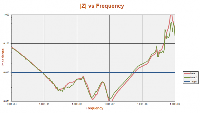
- What this plot shows is two different locations of connections when we measure the power distribution network. When you think about it, that is really the same thing as two different bypass capacitor placements relative to the chip.
For frequencies up to 250 MHz these two measurements are identical. In other words, bypass capacitor placement is NOT important.
Fussing over bypass capacitor placements may even make things worse because caps placed close to chips with high routing density will tend to block the routing forcing you to add layers.
This also explains why a simple tool like the PDN Tool is a good mechanism for selecting the right bypass capacitors for your design. The specific placement is not important, but the types and number of capacitors are important.
Important: When you don’t have a good solid power plane area, but rely on (even very fat) traces, this does not work. So just don’t do that and make your life easier 🙂 An example of this is the funky Zedboard we examined a while back.
 M.Sc.EE, SI Consultant
Hi Rolf!
Thank you for sharing your knowlege.
I believe you if you have a PCB with a very thin layer between the GND- and power- plane and the circuits closely connected to these planes with low serial inductance.
But sometimes are PCBs not that good and has not big power planes due to few layers and many different PDNs.
It’s interesting to compare your “Bypass cap location is irrelevant” with “28. Waves of Power Disturbance” in the EE Times corse “Fundamantals of PCB Design”.
BR / Bo Elm
Thanks for the comment. I found the section 28 of Howard Johnsons free 50 minute webinar you are referring to here: http://www.techonline.com/electrical-engineers/education-training/courses/4000356/fundamentals-of-pcb-design?isvalidated=1
And indeed the section 28 seem to go right against the measurements above. Funny. I based my blog post on actual measurements – not nice computer graphics though 🙂
When you talk about less than .3-.4ns you are talking about more than 1GHz – remember BW~0.35GHz @ 1ns rise time. It is very difficult for a discrete capacitor to effectively bypass your pwr/gnd planes at more than about 500 MHz due to the parasitic inductance. Also board resonances (which in effect is what Howard is really showing the beginning of on that slide) limits the practical effectiveness of the whole PDN to about 500MHz-1GHz. That is why bypass at those higher frequencies needs to happen at the package/die level.
What Howard forgets to show is how little effect a discrete bypass cap would have in that timescale – no matter where you place it.
As for the closely coupled and fairly solid power ground planes – yes, all my boards have that and the blog post stresses that assumption as well. Only for the super high volume 4-layer PC motherboard or something like that would it make sense for me to not do that. It’s just so much easier as you can see. Who pays for all the extra simulation and validation time when you go cheap and try to save a few layers?
Read more about on-die and on-package bypass here: https://www.ee-training.dk/announcement/how-much-bypass-does-the-zynq-have-on-chip.htm