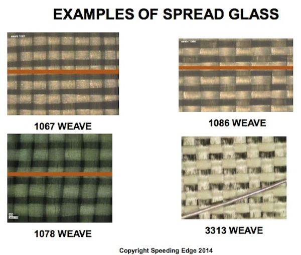
Spread glass is important. When designing 10+ Gbps systems, you may or may not be aware of how important the glass weaves are. You definitely should be. And getting it right is not easy. No real specifications to go by. No consistent information from the vendors and fabricators. Lots of information pointing in different directions.
There really is no other way than actually understanding the stuff. But that is not enough. You also need to know how it performs in real manufacturing processes.

A recent discussion on the premier email list on signal integrity: SI-LIST proves how difficult this subject is.
Our good friend Lee Ritchey does the right thing – unfortunately most of us can not afford that. He designs test boards and does actual measurements. We have access to all that data and use this in the training as well.
Spread glass is used instead of glass bundles in manufacturing of PCB’s for lots of high-speed designs today, but the materials were really developed for making a more even laser-drill process for cell phone PCB’s. It just happens to also be a very effective method of making sure the DK of prepregs and laminates is very uniform and consistent along the trace. And even more importantly: the same “local” DK for two traces of a high-speed differential pair.
Note: We cover glass weaves and how to optimally use spread glass in our 3-day Signal Integrity class as well as other issues to be aware of when designing systems for speeds from 5 Gbps to above 56 Gbps. All based on actual experience, test boards, and the associated theory.
 M.Sc.EE, SI Consultant