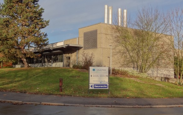
Another PCB factory tour. Two weeks ago, I finally got to visit Multek in Boeblingen near Stuttgart. Very interesting visit – as always when you visit a manufacturer you are using or is going to use. Generally, I prefer to go visit a manufacturer whenever I start doing business with them, but in this case, my client had actually been working with Multek for several years and never been to the plant. It turned out to be a very worthwhile visit on several levels.
 Multek is a part of Flextronics, which is one of the multinational big players in electronic manufacturing services. The plant in Boeblingen manufactures advanced printed circuit boards. That was exactly why my client wanted to work with Multek. Now the interesting thing to see at a factory tour is just how well the things you make matches the general picture of the products manufactured at the site.
Average layer count is 22
We were very impressed by what we saw – the average layer count is 22 at this factory. That is not by itself a very good way to measure neither quality or complexity, but it does tell you something. And walking around the huge manufacturing complex reinforced the impression. You see boards at different stages in the production, and if what you see looks similar to your own boards you know you may be in the right place.
We generally saw big thick boards with multiple 1500+ ball BGA’s, high layer counts (up to 40 was spotted), tons of laser drilling, back-drilling, via plugging and other sure signs that this is where some of the most advanced boards are being built for “big iron” networking products and some test & measurement type products. Another distinct type of boards spotted was for smallish medical type products, where quality and traceability is very important.
Back-drilling is moving forward
When you do a PCB factory tour, you typically have two things in mind. How is the quality/facility and how are the people? But usually, you learn something unexpected as well. One of the things we learned was that back-drilling is now so much mainstream for these advanced telecom boards that 50% of the boards had back-drilling.
Back-drilling is the process of removing the (unused) part of a via from the bottom side of the board with a slightly bigger drill. This is done as one of the last production steps after plating and via formation. The reason this matter is capacitance. Unused copper attached to a high-speed signal path in the form of a 2-3mm unused via end forms a capacitor to the surrounding copper. This excess capacitance creates reflections due to impedance mismatch.
So the forefront of high-speed signaling is now at a point where 50% of the boards at a place like Multek are back-drilled. We knew it was coming but at that speed? Somewhat of a surprise. That’s what we call learning.
Now you go visit your manufacturer
If you have not yet visited your PCB manufacturer – go book a date. It’s really worth it and for a number of reasons.
- As design engineers, we need to educate ourselves in board manufacturing techniques to understand the limitations and challenges. With technology advancing so fast, you need to constantly learn just to keep up.
- When working with a manufacturer – you are working with other real humans. Get to know them as people by meeting them face to face, and your communication will flow a lot better on email and phone afterward.
- See for yourselves if your manufacturer is really a good match for the types of boards you are doing. If you care, chances are they will care too.
If you want advice on what to look for when you do a factory visit, my friend Lee Ritchey has a 2002 article on the subject, that I still find quite useful.
The article actually talks about Multek at the very end, but I must say that the impression we got from our recent visit was that of a highly capable and quality-focused manufacturer doing some of the most advanced boards in the industry. Note however that Multek is a brand and covers multiple factories with a different focus.
I wish you good luck and let us all know if you learned something new from your PCB factory tour?
 M.Sc.EE, SI Consultant
Flextronics just announced they are closing down this plant. Sad to see as it was definitely a good place in EU to have very advanced boards build. On the other hand I am sure it opens new and interesting opportunities for all the talented workers in the area.