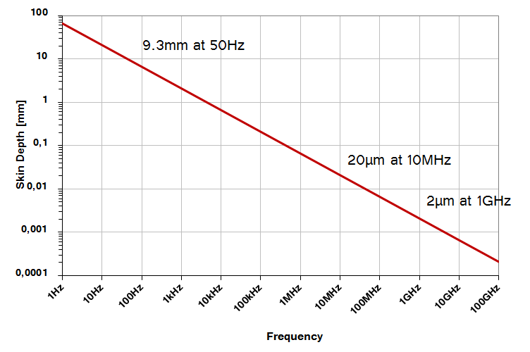
Skin-effect pushes the current to the outer part of any metal conductor, which is why we need to worry about Cu roughness. For copper, as it is used on a printed circuit board (PCB) the effective skin depth goes like this over frequency.
 With signaling speeds on PCB going to 28 Gbit/s (example: FPGA’s in 2013) and beyond, the effective skin depth gets to sub-micron thickness. This is why the roughness of the copper (few to several microns) used to form traces on a PCB start to matter a lot.
And to make matters worse – copper roughness it not only defined by the laminate manufacturer (as Lee Pangier explained in this video) but also by the board manufacturer.
From the 2012 Copenhagen class of Stackup Design, Lee Ritchey here explains this by use of an example board manufactured by two different manufacturers. One passes – the other fails, with exact same materials and stackup.
Fun is certainly not over for those doing high-speed electronic designs today.
Cu roughness is – depending on the copper foil specified – in the range of 1-5um. By looking at the graph above, it’s clear that this is clearly in the range where the 5+ Gbps signals will be affected. Specifying copper right is important for any stackup that handles such fast signals. Also, see Lee Ritchey’s top 5 tips for dealing with surface conductor roughness.
There is more about Cu roughness and all the other important things in our 3-day Signal Integrity with Hands-On courses.
 M.Sc.EE, SI Consultant